NP-1 “Apex” — Neural Inference Accelerator
4 nm neural-processor for sustained on-device inference. Runs transformer and convolutional workloads at the edge — no host offload, no network round-trip. All figures are engineering-silicon measurements or nominal-condition peaks.
Table 1. NP-1 “Apex” electrical characteristics — nominal voltage, 25 °C, PeakStack 3.2.
| Parameter | Value | Unit |
|---|---|---|
| INT8 throughput UP TO | 512 | TOPS |
| FP16 / BF16 throughput UP TO | 256 | TFLOPS |
| FP4 / INT4 throughput UP TO | 1,024 | TOPS |
| On-chip SRAM | 96 | MB |
| External memory bandwidth | 256 | GB/s |
| Power TYP | 85 | W |
| Process node | 4 | nm |
| Package | 45×45 | mm FC-BGA |
Notes: “up to” = peak at nominal voltage; “typical” = measured on engineering silicon under sustained full utilization. Specifications are preliminary and may change before production release. Full conditions in NP1-DS-001.
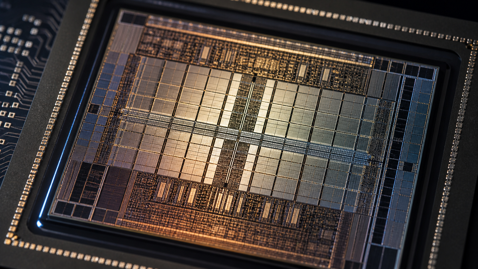
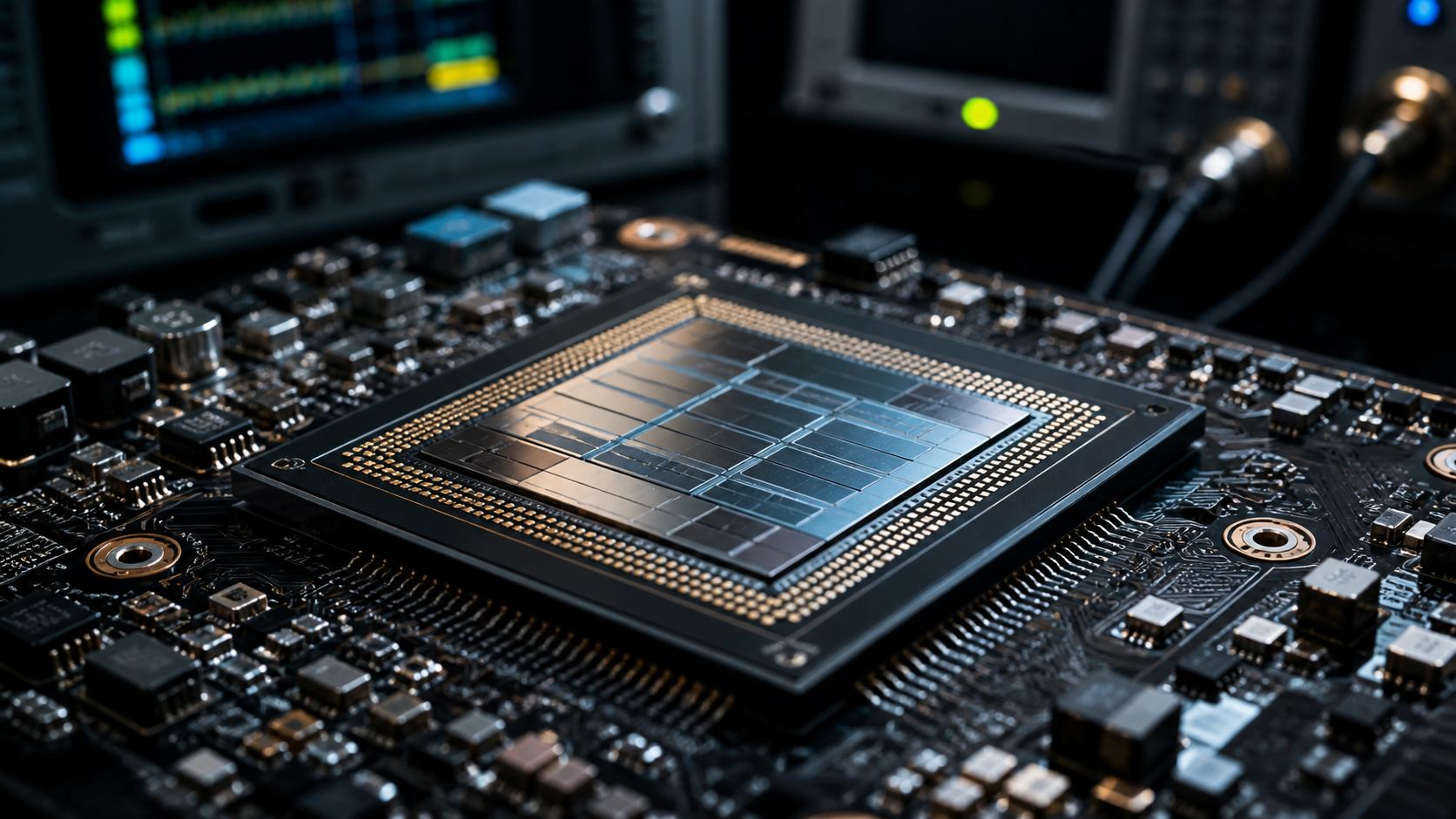
2. Product line — one instruction set, three parts
All parts share the same ISA and the PeakStack toolchain; a model compiled for NP-4 runs on NP-1 unchanged.
Table 2. Line summary.
| Parameter | NP-1 Apex | NP-2 Crest | NP-4 Ridge |
|---|---|---|---|
| INT8 (dense) | 512 TOPS | 128 TOPS | 8 TOPS |
| FP16 / BF16 | 256 TFLOPS | 64 TFLOPS | 4 TFLOPS |
| FP4 / INT4 | 1,024 TOPS | 256 TOPS | 16 TOPS |
| On-chip SRAM | 96 MB | 32 MB | 4 MB |
| External memory | LPDDR5X · 256 GB/s | LPDDR5 · 128 GB/s | QSPI/OSPI flash |
| Power (typical) | 85 W | 20 W | 1.2 W |
| Process | 4 nm | 6 nm | 12 nm |
| Package | 45×45 mm FC-BGA | 21×21 mm FC-BGA | 12×12 mm QFN-88 |
Full per-part datasheets: NP1-DS-001 · NP2-DS-002 · NP4-DS-004.
3. Measured performance — throughput on engineering silicon
Table 3. Reference results (batch 1 unless noted).
| Workload | NP-1 | NP-2 | NP-4 |
|---|---|---|---|
| ResNet-50 (batch 64) | 48,000 img/s | 12,000 img/s | 1,800 img/s |
| YOLOv8n (batch 1) | 1,650 fps | 420 fps | 55 fps |
| Llama-3-8B decode (INT4) | 180 tok/s | 55 tok/s | 8 tok/s |
| Llama-3-8B prefill (INT4) | 12,400 tok/s | 3,900 tok/s | 620 tok/s |
NP-4 rows are pre-silicon targets; NP-1/NP-2 measured on engineering silicon. Full methodology in Performance.
4. Architecture — a memory-bound design, by intent
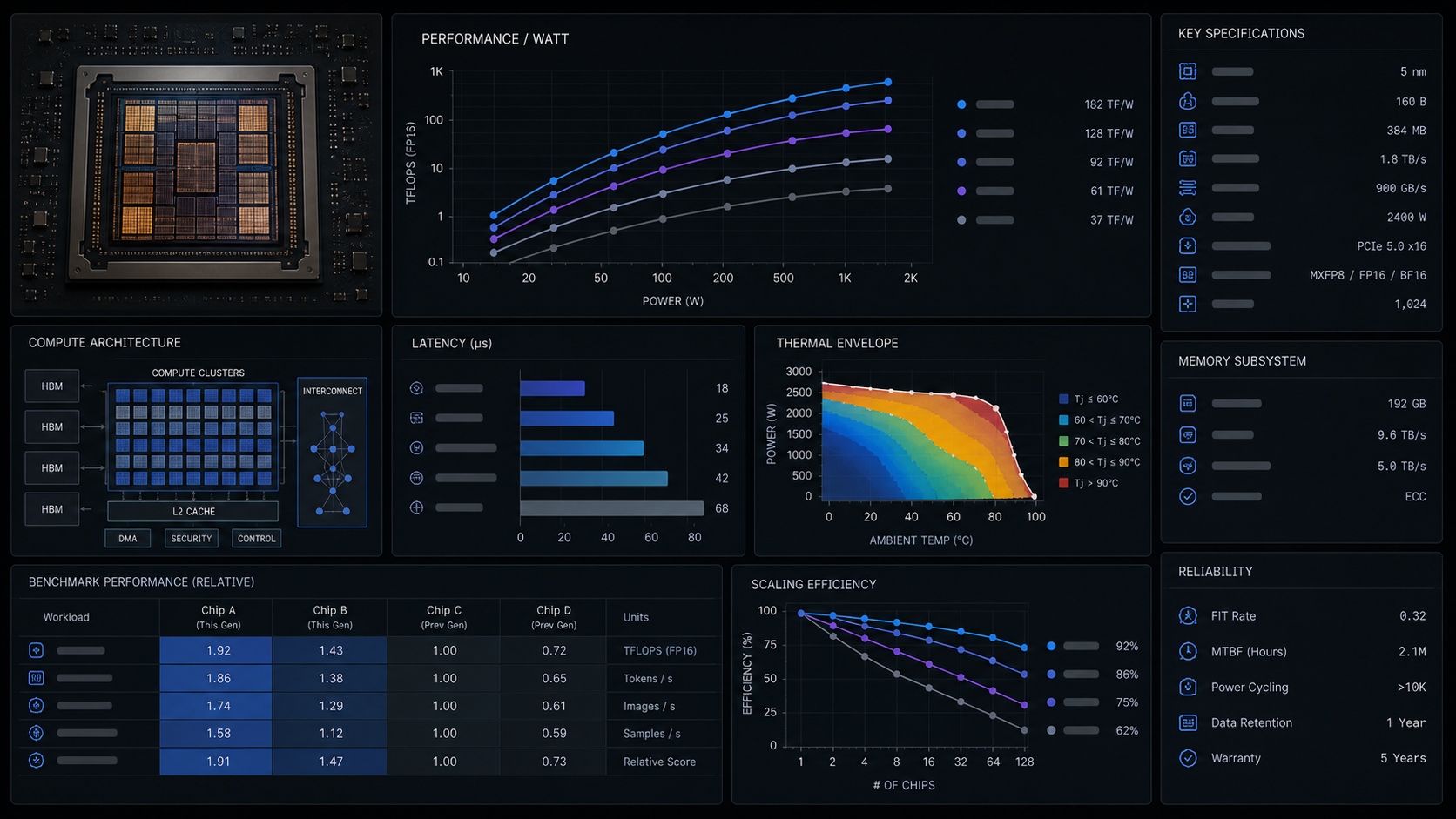
The memory wall, not compute, bounds most edge-inference latency. NP-1 keeps weights resident in on-chip SRAM so the MAC array never waits on an external bus.
5. Thermal & packaging — FC-BGA with integrated heat spreader
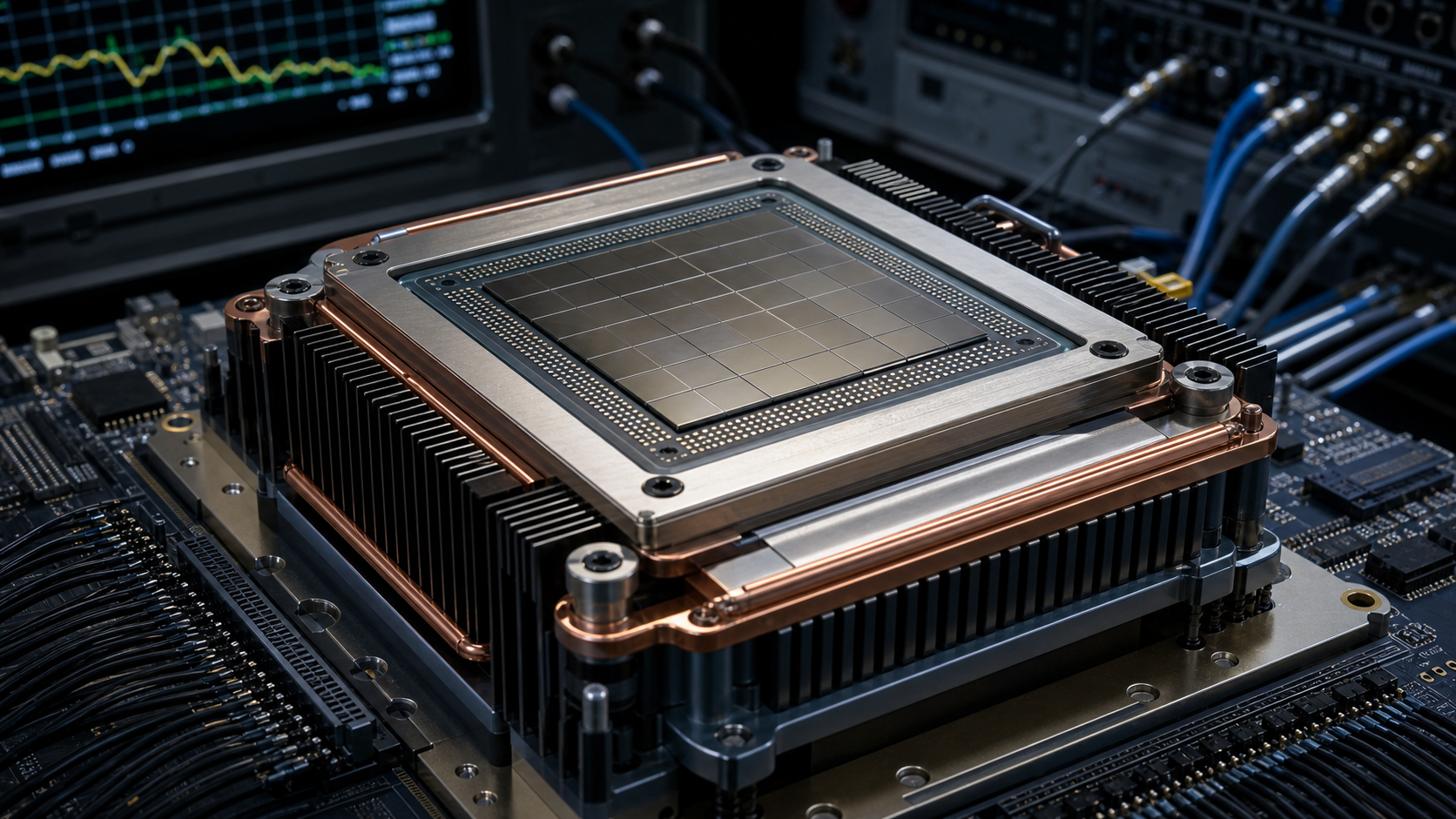
The 45×45 mm FC-BGA package routes 2,116 balls at 0.5 mm pitch and carries an integrated heat spreader to sustain full-load operation within the 85 W typical power envelope.
6. Whitepapers — gated to design partners
Abstracts are public; full documents are distributed under NDA to registered design partners.
| Code | Title | Rev | Date |
|---|---|---|---|
| WP-001 | NP-1 Architecture Overview | 1.2 | 2026-08 |
| WP-002 | Structured Sparsity in PeakStack | 1.0 | 2026-06 |
| WP-003 | INT4 / FP4 Quantization Methodology | 1.1 | 2026-05 |
| WP-004 | The PeakStack Compiler: from ONNX to Silicon | 2.0 | 2026-04 |
| WP-005 | Memory Subsystem and Dataflow | 1.0 | 2026-03 |
Complete index and SDK reference in Resources.
7. Document history — announcements & revisions
PeakStack 3.3 — FP4 sparsity kernels and ONNX Runtime bridge
2:4 structured-sparsity kernels now cover FP4; new scheduler pass for the 2-D mesh; drop-in ONNX Runtime execution provider.
NP-2 “Crest” reaches general availability
Mid-range part moves from sampling to GA across commercial and industrial temperature grades.
NP-1 first silicon boots; bring-up complete
Functional bring-up across the full die: PCIe, memory PHY, and all 16 processing elements.
Versioned toolchain changelog and silicon revisions in Announcements & Changelog.